

📊 Full opportunity report: The Learning-by-Doing Strategy Fueling China’s AI Rise on ThorstenMeyerAI.com — validation score, market gap, and execution plan.
TL;DR
China is making significant progress in AI hardware and manufacturing, driven by a learning-by-doing strategy. While initial prototypes exist, scaling reliable, high-yield production remains a complex, long-term challenge. This approach marks a phase transition in China’s tech development.
China has begun mass-producing domestically developed immersion DUV lithography machines and is prototyping EUV tools, marking tangible progress in its chip manufacturing capabilities. This shift is significant as it demonstrates China’s move from reliance on foreign technology toward building its own advanced semiconductor infrastructure, which is crucial for its AI hardware ambitions.
Multiple credible sources confirm that China is now manufacturing domestic immersion DUV lithography machines capable of producing chips at 28-nanometer nodes, with potential to reach 5- to 7-nanometer nodes through multi-patterning. SMIC, China’s leading foundry, has demonstrated 7-nanometer production using older DUV tools, and reports suggest ongoing development of 5-nanometer capabilities. Additionally, Reuters reports that China is at the prototype stage of its domestic EUV machine, an advanced tool critical for next-generation chip manufacturing.
Despite these technological strides, significant hurdles remain. Yield rates for China’s 5-nanometer chips are around 20 percent, compared to the industry standard of approximately 90 percent. China relies heavily on imported high-purity materials, such as photoresist, predominantly sourced from Japan. Experts estimate that China’s domestic DUV tools lag behind the leading edge by roughly four generations, with commercial sub-10-nanometer production not expected before 2030. Furthermore, the existing installed base of advanced DUV tools depends on Western servicing and maintenance, which China cannot yet fully control.
Every few weeks a headline says China cracked the last hard problem in chipmaking — and triggers alarm in one camp, triumph in the other. Both overreact, because both mistake a learning-by-doing problem for a copying problem. It isn’t one.
▲ Forward-looking · figures are point-in-time estimates“A machine exists” and “a machine makes advanced chips at scale, profitably, for years” are separated by a chasm — made of things that only accumulate with time.
In a race, a burst of speed closes the gap. In a phase transition, you can’t move faster to cross over — you have to accumulate enough, slowly, until the system changes state.
When you see “China achieves X,” ask which of two very different claims is actually being made.
Even amid the loud headlines, the quiet data points all say the same thing.
No prototype, no shipped tool, no yield headline teleports past it.
Implications of China’s Incremental Semiconductor Progress
This development signifies a strategic shift for China, emphasizing a long-term, learning-driven approach to mastering advanced chip manufacturing. While initial prototypes and limited production exist, achieving reliable, high-yield, commercial-scale manufacturing remains a complex challenge. This approach reflects a phase transition in China’s technological capabilities, focusing on accumulating tacit knowledge through iterative process improvements rather than quick technological leaps.
The progress impacts global supply chains, U.S.-China tech competition, and the future of AI hardware development. It underscores that China’s advancements are not solely about acquiring foreign technology but about building an indigenous ecosystem through sustained, incremental learning, which could reshape the global semiconductor landscape over the next decade.

The Semiconductor Manufacturing Business: A Comprehensive Guide
As an affiliate, we earn on qualifying purchases.
As an affiliate, we earn on qualifying purchases.
China’s Semiconductor Development Timeline and Challenges
Over the past decade, China has prioritized developing its semiconductor industry amidst export controls and technological restrictions. Initial efforts focused on copying foreign designs, but recent progress shows a shift toward domestic innovation. The country has achieved some success with older node production and is now working on advanced tools like EUV lithography, which are critical for scaling down chip sizes. However, experts agree that China remains at least four generations behind industry leaders like ASML, and commercial viability of sub-10-nanometer chips domestically is still years away.
This progress is part of China’s broader strategy to reduce dependence on foreign suppliers, especially for high-end materials and equipment, which remains a significant bottleneck. The reliance on imported photoresist and the servicing dependency on Western firms highlight ongoing vulnerabilities in China’s supply chain.
"China’s progress in domestic lithography is real, but the gap in yield, materials, and know-how remains substantial. Achieving reliable, large-scale production is a long-term process of accumulated learning."
— Thorsten Meyer

Resiners Resin Curing Machine G3 with UV Resin Light, 2H/1Min Fast Curing, Silicone Mat Included, Deformation-Resistant Reversible Base, Resin Dryer for Epoxy Mold Casting, Jewelry Making, DIY Decor
- Fast Curing for Epoxy & UV Resins: Cures epoxy in 2 hours, UV in 1 minute
- Uniform and Even Curing: Reversible high-temp resistant base with thermal cycle
- Dual-Wavelength UV Light: 365nm+395nm UV for optimal curing
As an affiliate, we earn on qualifying purchases.
As an affiliate, we earn on qualifying purchases.
Uncertainties in China’s Semiconductor Capabilities
It remains unclear how quickly China can improve yield rates from 20 percent toward industry standards, and whether domestic materials supply chains can be fully localized without reliance on imports. The timeline for achieving commercial sub-10-nanometer production domestically is uncertain, with estimates extending into the early 2030s. Additionally, the extent to which China can develop independent servicing and maintenance capabilities for advanced lithography tools is still unresolved.
high-purity photoresist for chipmaking
As an affiliate, we earn on qualifying purchases.
As an affiliate, we earn on qualifying purchases.
Next Steps in China’s Semiconductor Development
China is expected to continue incremental improvements in yield and materials purity, with ongoing development of EUV prototypes and efforts to domesticate supply chains. Industry experts anticipate that commercial-scale production at sub-10-nanometer nodes domestically may not occur before 2030, but progress in process refinement and materials will be critical milestones. Monitoring government policies and industry investments will be essential to gauge the pace of China’s technological maturation.
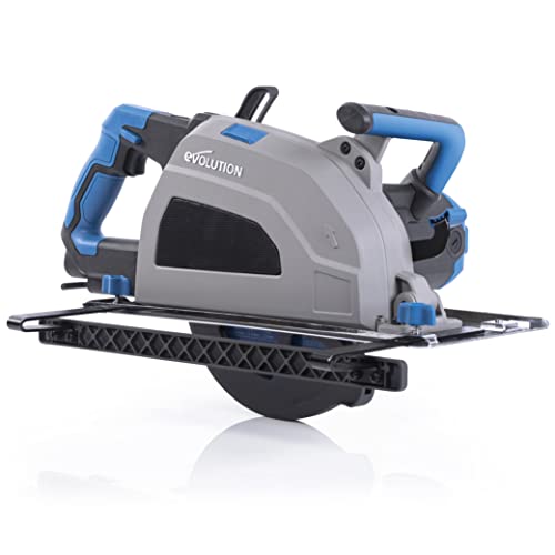
Evolution S210CCS Metal Cutting Circular Saw | 8-1/4" Blade | Cuts Steel Clean & Cool | Adjustable 3" Depth | Chip Collector | No Heat Burr or Sparks | High Torque Motor | TCT Blade Included
- Blade Type: TCT blade included for clean cuts
- Cutting Capacity: Cuts steel up to 1/2 inch thick
- Cutting Performance: Fast, cool, burr-free steel cutting
As an affiliate, we earn on qualifying purchases.
As an affiliate, we earn on qualifying purchases.
Key Questions
How advanced are China’s current chip manufacturing tools?
China has domestically produced immersion DUV lithography machines capable of 28-nanometer production, with ongoing development of EUV prototypes. However, their tools lag behind industry leaders like ASML by about four generations, and commercial sub-10-nanometer production is still years away.
What are the main challenges China faces in advancing its chip manufacturing?
Major challenges include low yield rates (~20%), dependence on imported high-purity materials like photoresist, lagging equipment technology, and reliance on Western servicing for advanced lithography tools. Overcoming these will require years of process refinement and supply chain localization.
Why is the learning-by-doing approach significant for China’s tech rise?
This approach emphasizes accumulating tacit knowledge through repeated process runs, which is essential for mastering complex manufacturing at scale. It indicates that China’s progress depends on long-term, incremental process improvements rather than quick technological fixes.
When might China achieve independent, commercial sub-10-nanometer chip production?
Most credible forecasts suggest this milestone could be reached around 2030, contingent on overcoming yield, materials, and equipment development challenges.
Source: ThorstenMeyerAI.com